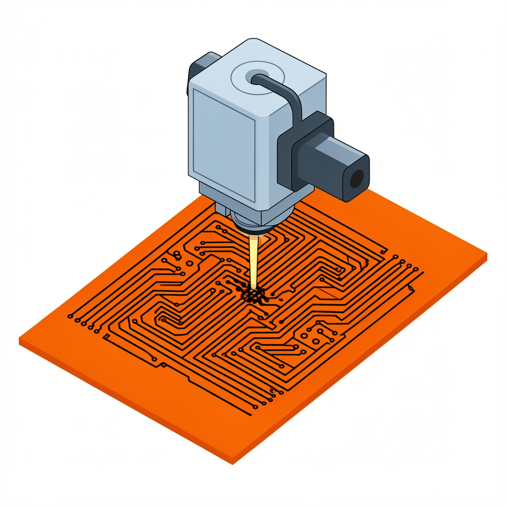
A DIY-compatible, low-cost method for producing conductive carbon electronics on Kapton tape using a desktop laser engraver.
Abstract
The development of printed two-dimensional circuits is becoming crucial for next-generation electronics. Demand for biocompatible, flexible circuits has driven interest in carbon-based fabrication methods. We present a simple method for producing laser-induced graphene (LIG) circuits on Kapton tape using a low-cost desktop laser engraver (LaserPecker 3). A mechanically abraded Kapton sheet is patterned with a vector design, converting exposed regions into conductive graphene. Resistances as low as 8 Ω/mm² were obtained with two writing passes at 1k resolution and a focal distance of 14.2 mm. This note summarizes the setup, the relevant laser parameters, the governing formulas, and the experimental results.
Background
Laser-induced graphene is a three-dimensional, porous carbon nanomaterial produced by irradiating carbon-rich precursors with a laser—typically a CO2 laser—in ambient air. First demonstrated in 2014 at Rice University by Lin, Tour & co-workers, the photothermal process converts the sp3 carbon of polyimide directly into sp2 graphene networks without additional chemical reagents [1]. The resulting porous film is bonded to the polymer substrate, so it can be patterned in a single, mask-free step by simply rastering the laser beam.
The dominant mechanism is photothermal conversion: laser absorption heats the polymer locally above its decomposition temperature, releasing nitrogen and oxygen while reorganizing the remaining carbon into defective, few-layer graphene sheets. By adjusting laser wavelength, fluence, scanning speed and atmosphere, the resulting morphology can be tuned from isotropic porous structures to anisotropic cellular or woolly fibers. This customization permits control of electrical conductivity, capacitance, wettability and surface area, yielding flexible electrodes with thicknesses on the order of tens of microns.

Applications in the literature
Because LIG can be produced on flexible polymer films in ambient air with no wet chemistry, it has become a platform material for low-cost electronics. Reported applications include in-plane microsupercapacitors with specific capacitances above 4 mF cm−2 [1], electrochemical sensors for heavy metals and metabolites [2], strain and pressure sensors for rehabilitation monitoring [3], thermoelectric foams for self-powered sensing [4], and laser-healed conductive traces with improved crystallinity [5]. More recent work has also transferred LIG onto elastomers as thin as 6.7 µm for large-area electronic skins [6]. These diverse uses all exploit the same core advantage: a conductive, high-surface-area carbon layer generated in a single laser-writing step.
Experimental Methods
- Substrate preparation
- Kapton sheets were cut into 40 mm × 40 mm squares. Surfaces were mechanically abraded with fine sandpaper to promote graphene and porous-structure formation, then cleaned with ethanol to remove contaminants that could lead to inhomogeneous conversion.
- Fabrication setup
- After 5 minutes of air drying, each sample was secured with Kapton tape to the bottom plate of a LaserPecker 3 laser engraver. The print area was aligned to the top-left corner of the software preview.
- Parametric screening
- A series of laser passes were executed at varying depth/power percentages, focal distances, resolutions, and pass counts to identify the processing window that yields conductivity.

Process Parameters and Formulas
| Symbol | Description | Units / Remarks |
|---|---|---|
| P | Laser power | W |
| P(%) | Relative power setting | Fraction or % |
| β / βmax | Beam-width ratio | Dimensionless |
| f / # | Optical F-number | Dimensionless |
| h | Hatch spacing (line spacing) | µm (convert to mm for energy-density calculations) |
| Res | Resolution code | e.g., 1k, 2k, 4k |
| S | Scan speed | mm/s |
| Smax | Max scan speed at given resolution | mm/s |
| Depth(z) | Process depth / penetration | Reciprocal of Smax as written |
| Dep | Depth factor | Dimensionless |
| Ed | Areal energy density | J/mm² |
| D | Duty cycle | % |
| Category | Expression | Notes |
|---|---|---|
| Power scaling | P(%) = (β / βmax) · (f / #) | Annotated “pwr width (ns)”; pulse-width dependence is noted but unspecified. |
| Full-power reference | P(100%) = 1 W | 100 % scale = 1 W. |
| Hatch spacing | h = (1 / Res) · 100 µm | — |
| Speed limits |
Smax(1k) = 800 mm/s Smax(2k) = 400 mm/s Smax(4k) = 200 mm/s |
Units: mm/s. |
| Depth (reciprocal) | Depth(z) = 1 / Smax(Res) | Written as a direct reciprocal; a proportionality constant may be required. |
| Depth factor | Dep = 100 / Res | Used in the LCD shortcut. |
| Energy density (full) | Ed = P / (S · h) | Use consistent units: P [W], S [mm/s], h [mm]. |
| Energy density (LCD) | Ed = P(%) · Dep | Shortcut valid when parameters are aligned to the full formula. |
Results
| Depth (%) | Power (%) | Focus (mm) | Conductive | Resistance (Ω/mm²) | Passes | Resolution |
|---|---|---|---|---|---|---|
| 100 | 80 | 13.8 | No | — | 1 | 1k |
| 100 | 100 | 13.8 | No | — | 1 | 1k |
| 100 | 100 | 14.5 | No | — | 1 | 1k |
| 100 | 100 | 13.0 | No | — | 1 | 1k |
| 100 | 100 | 14.8 | No | — | 1 | 1k |
| 100 | 100 | 15.2 | No | — | 1 | k |
| 100 | 100 | 14.2 | Yes | 8 | 2 | 1k |
| 20 | 100 | 14.2 | Yes | 20 | 2 | 4k |
Discussion
The parametric sweep reveals that conductive traces were achieved only at a focal distance of 14.2 mm, using 2 passes at 1k resolution and 100 % power. At focal distances between 13.0 mm and 15.2 mm—regardless of power or depth percentage—no conductivity was observed with single-pass processing at 1k resolution. Sheet resistance values of 8 Ω/mm² and 20 Ω/mm² were recorded for 100 % and 20 % depth settings, respectively, indicating that once the focal window and resolution are correct, the depth percentage modulates the final resistance.
Key insight. These results suggest that the areal energy density must exceed a threshold to drive complete photothermal conversion of polyimide to graphene.

Conclusion
This note demonstrates a simple, DIY-compatible route for fabricating laser-induced graphene circuits on Kapton tape using a desktop laser engraver. By clarifying the relevant process parameters and formulas, and by identifying the critical focal distance and resolution required for conductivity, this work provides a reproducible starting point for producing low-cost, flexible, and biocompatible carbon electronics.
References
- J. Lin et al., “Laser-induced porous graphene films from commercial polymers,” Nat. Commun. 5, 5714 (2014). DOI: 10.1038/ncomms6714
- K. H. Chen et al., “Understanding Baseline Drift in Laser-Induced Graphene Electrodes and Its Impact on Heavy Metal Detection by Anodic Stripping Voltammetry,” J. Electroanal. Chem. (2026). PMID: 42182954
- L. Huang & N. Zhao, “Laser-Induced Graphene-Polyimide Film Sensor for Simultaneous Lip Electromyography and Pressure Monitoring in Personalized Rehabilitation,” J. Vis. Exp. (2026). PMID: 42149837
- L. Yang et al., “Thermoelectric porous laser-induced graphene-based strain-temperature decoupling and self-powered sensing,” Nat. Commun. 16, 1–12 (2025).
- “Flash healing of laser-induced graphene,” Nat. Commun. 15, 1–11 (2024).
- Y. Lu et al., “Universal modulus-free transfer of scalable laser-induced graphene for electronic skins,” Nat. Commun. 17, 1–12 (2026).